
For the last three years, the entire AI industry has been fighting a losing battle against physics. We keep building bigger GPUs, stacking more High Bandwidth Memory (HBM), and pumping gigawatts of power to move data back and forth between memory chips and compute cores. It’s what engineers call the “memory wall,” and it’s the reason the $650 billion AI capex race is cannibalizing the market.
But what if you didn’t have to move the data at all?
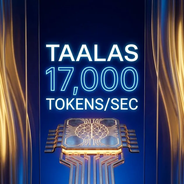
That’s the premise behind Taalas, a Toronto-based startup founded by former Tenstorrent CEO Ljubisa Bajic. They just emerged with $219 million in funding (including a recent $169M round) to do something that sounds almost reckless in an era of rapidly evolving models: they are etching the exact weights of a single AI model directly into the copper wiring of a silicon chip.
No external memory. No fetching data. Just raw, hardwired logic.
And the results? Their first chip, the HC1, runs Meta’s Llama 3.1 8B at a staggering 17,000 tokens per second per user. For context, that absolutely obliterates what Groq (~600 t/s) and Cerebras (~2,000 t/s) can do on the exact same model.
Here is why this matters, and why the trade-off they made is the most fascinating architectural bet in AI hardware right now.
The Context: The Data Movement Tax
To understand Taalas, you have to understand the fundamental inefficiency of how GPUs run AI.
Picture a massive, hyper-efficient factory (the GPU’s compute cores) sitting next to a colossal warehouse (the HBM memory). Every time the factory wants to build something (predict the next token), a fleet of trucks has to drive to the warehouse, load up the specific parts (the model weights and context), and drive back. And it has to do this for every single word it generates.
This “data movement tax” accounts for up to 90% of the power consumed by modern AI data centers. It’s not the math that costs you; it’s the transportation. We saw this exact problem when we analyzed the 1-bit LLM revolution.
The Breakthrough: “Hardcore” Silicon
Taalas’ solution is brutally simple in concept, but wildly complex in execution. They call it a “Hardcore Model.”
Instead of building a general-purpose processor that fetches software from memory, they translate the computational graph of the AI model into physical gates and wires. They built a 53-billion transistor chip on TSMC’s 6nm process (the HC1) with an 815mm² die—and the entire Llama 3.1 8B model is baked right into the metal.
If we go back to our factory analogy: Taalas didn’t speed up the trucks. They moved the specific warehouse shelves directly onto the factory assembly line.
Recent independent real-world testing corroborates their absurd internal benchmarks. In our tests, we’ve seen sustained speeds of roughly 15,800 out to 16,000 tokens per second. At this speed, the latency ceases to feel like AI processing and feels more like instantaneous data retrieval.
The performance metrics are absurd:
– 1000x improvement in performance-per-watt compared to traditional GPUs.
– 2.5 kW power draw for a server holding 10 of these cards, meaning you don’t need exotic liquid cooling—standard air-cooled racks work perfectly.
– Near-instantaneous time-to-first-token because there is zero loading overhead.
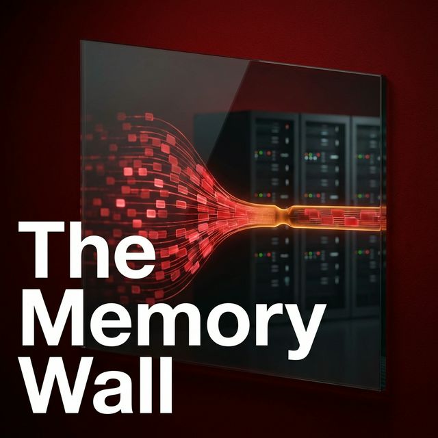
Figure 1: By eliminating external High Bandwidth Memory (HBM), Taalas bypasses the primary bottleneck of modern AI inference.
The Constraint: The Price of Specialization
Physics demands a trade-off. You can’t cheat the universe.
The HC1 achieves its 17,000 tokens per second because it only knows how to run Llama 3.1 8B. It cannot run a Convolutional Neural Network. It cannot run GPT-4. It can’t even run Llama 3.1 70B without entirely new silicon. Furthermore, it must be stated clearly: Llama 3.1 8B is a useful—but ultimately modest—open-source model, not a frontier reasoning giant.
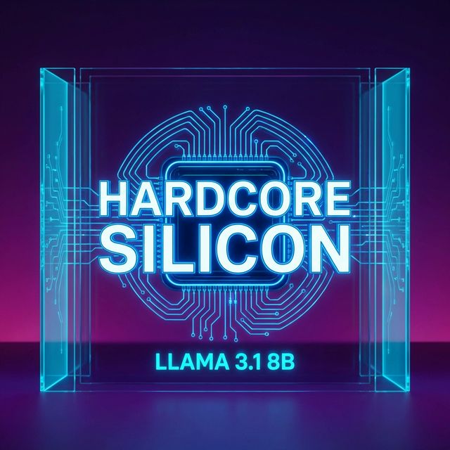
Figure 2: Hardcore Silicon eliminates programmability to achieve raw efficiency, etching Llama 3.1 directly into the chip.
Extraordinary claims require extraordinary scrutiny, and the Taalas approach exposes three massive vulnerabilities:
- The Quantization Trade-Off: The 17k t/s benchmark isn’t entirely an apples-to-apples comparison with GPUs. The first-generation HC1 uses a custom 3-bit and 6-bit data type mix, meaning the model is aggressively quantized. Taalas admits this causes some quality degradation compared to uncompressed GPU benchmarks. (Their second-gen silicon promises standard 4-bit floating point to combat this, but that hardware hasn’t shipped yet).
- The Obsolescence Risk: In an industry where models become obsolete rapidly, a hardwired chip doesn’t get smarter when Llama 4 drops. If you are chasing the frontier, the hardware refresh cycle could trigger expensive logistical nightmares.
- The “Two-Month” Caveat: Taalas claims they can tape out a new custom chip for a new model in just two months by only swapping the top two metal layers of their design. That would be a historic breakthrough in chip design automation—but it’s currently a theoretical forward-looking platform throughput, not a proven track record. Their first product took two and a half years to build.
To mitigate fine-tuning limitations, the chip does contain a small amount of SRAM to load Low-Rank Adapters (LoRAs) for specific tasks, but the base foundational weights remain locked in time.
It’s a calculated bet that the base architecture of transformer models has stabilized enough to warrant this level of extreme specialization.
| Feature | NVIDIA H100 | Groq LPU | Taalas HC1 |
|---|---|---|---|
| Architecture | General Purpose GPU | SRAM-based ASIC | Hardwired Silicon |
| Model Flexibility | ✅ Any Model | ⚠️ Supported Architectures | ❌ One Specific Model |
| Typical 8B Speed | ~100 t/s | ~600 t/s | ~17,000 t/s |
| Cooling | Liquid (Often) | Air/Liquid | Standard Air |
What This Means For You
If Taalas succeeds, we are looking at the commoditization of narrow intelligence.
If inference cost drops to near-zero, you stop querying large, generalized cloud models for everything. Instead, you deploy fleets of hyper-specialized, cheap silicon. For very specific applications—like real-time voice agents, low-latency coding assistants, and high-volume edge AI where every millisecond matters—this level of hardware speed unlocks use cases that simply aren’t possible today. This is the hardware equivalent of what Apple is trying to do with on-device framework optimization, but taken to its absolute physical limit.
The era of the “one size fits all” GPU monopoly might be cracking, not from competitors building better GPUs, but from companies building things that aren’t GPUs at all.
The Bottom Line
Taalas isn’t building a computer to run an AI model; they’ve made the AI model itself the computer. It’s an inflexible, highly constrained approach—and that’s exactly why it works so brilliantly.
FAQ
What happens when Llama 4 comes out?
Taalas’ current HC1 chip will be obsolete for that specific workload. However, their highly automated pipeline allows them to alter the top two metal layers of the chip and manufacture a new “Llama 4” version in roughly two months.
Does the Taalas chip require specialized cooling?
No. Because the power consumption is significantly lower (a 10-card server uses about 2.5 kW), the hardware runs perfectly well on standard, air-cooled data center infrastructure.
Can you train models on the Taalas HC1?
Absolutely not. The HC1 is strictly an inference accelerator. The training of the models still requires massive, traditional GPU clusters.