
For years, the conventional wisdom was simple: China can’t make advanced chips because ASML won’t sell them EUV machines.
That assumption just got a lot more complicated.
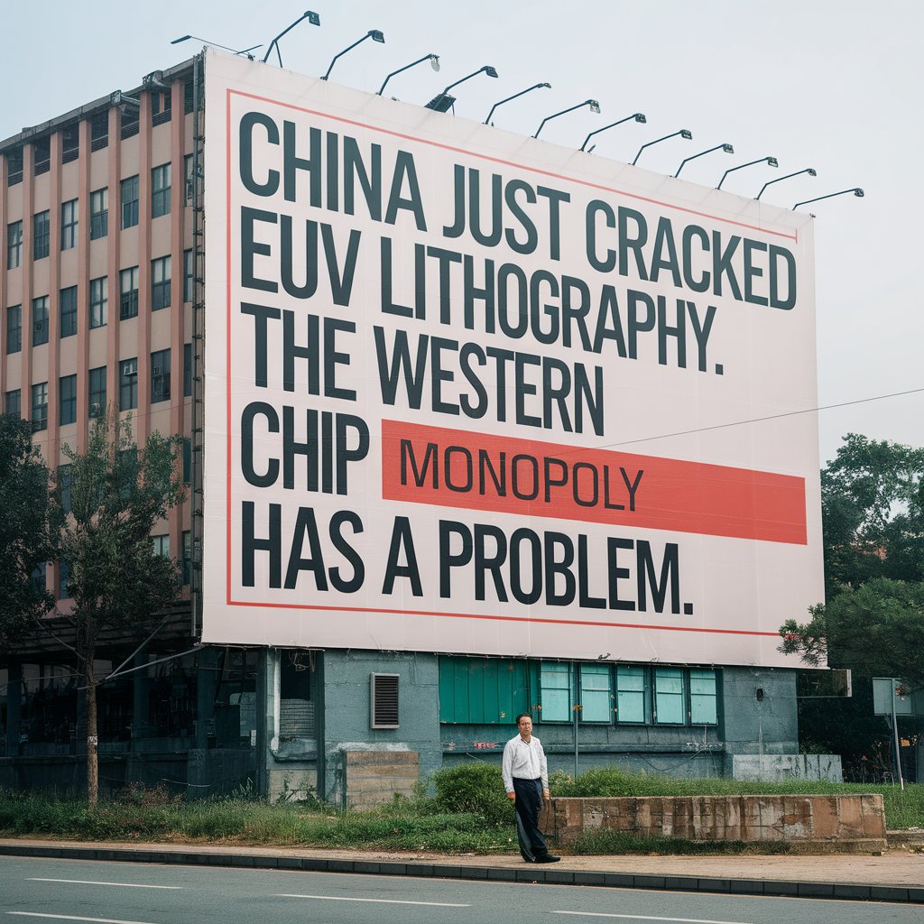
According to multiple reports, a working EUV lithography prototype is now being tested at a high-security facility in Shenzhen. It’s not producing chips yet. But it’s generating extreme ultraviolet light—the fundamental first step toward breaking the Western semiconductor monopoly.
This is China’s Manhattan Project moment for chips. And whether you’re bullish or bearish on Chinese tech, you need to understand what’s happening.
What EUV Lithography Is (And Why It Matters)
Extreme Ultraviolet lithography is the technology that makes chips below 7nm possible. Without it, you can’t manufacture the processors that power iPhones, data centers, or AI training clusters.
Here’s the physics: EUV uses light at 13.5nm wavelength—about 15 times shorter than the deep ultraviolet (DUV) light used in older processes. Shorter wavelengths mean finer patterns on silicon, which means more transistors per chip.
ASML, the Dutch company that has a literal monopoly on EUV machines, has spent decades perfecting this. A single machine costs $200+ million. ASML sells maybe 50 per year. Every advanced chip on the planet traces back to their technology.
When the US, Netherlands, and Japan blocked EUV sales to China in 2023, it was supposed to cap Chinese chip technology at 7nm forever.
The Two Paths to EUV Light: LPP vs. LDP
To understand what China is building, you need to understand the physics.
Laser-Produced Plasma (LPP) — ASML’s Method
This is the industry standard. ASML’s process:
1. Fire high-power lasers at microscopic droplets of molten tin in a vacuum chamber
2. A pre-pulse laser vaporizes the tin
3. A pulsed infrared CO2 laser irradiates the vaporized tin, creating high-temperature plasma
4. The plasma emits 13.5nm EUV light
This process is extremely precise, stable, and produces the consistency needed for 5nm and 3nm node manufacturing.
Laser-Induced Discharge Plasma (LDP) — China’s Alternative
China chose a different approach:
1. Evaporate a small amount of tin between electrodes (sometimes using a pre-pulse laser)
2. Ionize the tin vapor into plasma through a high-voltage electrical discharge
3. The collision of electrons and high-valence tin ions radiates 13.5nm EUV light
Why LDP? Proponents claim simpler architecture, smaller footprint, better energy efficiency, and lower production costs. Some experts speculate it could even exceed ASML’s LPP efficiency.
The catch: LDP was largely abandoned by Western developers in favor of LPP because LPP showed greater commercial promise at the time. China is essentially reviving a path the industry set aside.
What China Has Built
Based on reports from TrendForce, NotebookCheck, and other sources, here’s what we know:
The Shenzhen Prototype
A functional EUV prototype is undergoing testing at a secure facility. The system:
- Generates 13.5nm EUV light successfully
- Uses a Laser-induced Discharge Plasma (LDP) approach (different from ASML’s Laser-Produced Plasma method)
- Has not yet produced working chips
Huawei’s Coordination Role
Huawei is reportedly the central player coordinating this development. Their Dongguan facility is testing an LDP-based system that could serve as an alternative to ASML’s architecture.
This isn’t surprising. Huawei has been cut off from advanced chips since 2020, giving them maximum incentive to solve the problem domestically.
The Reverse Engineering Factor
Multiple reports acknowledge that Chinese engineers have studied existing ASML machines extensively. Combined with recruitment of former ASML employees (which has been documented), China has had access to significant institutional knowledge.
But here’s the nuance: EUV isn’t just about knowing how it works. It’s about precision manufacturing at extreme tolerances. The optics alone require Carl Zeiss AG’s expertise—expertise that isn’t easily replicated.
The Timeline Reality
Let me temper the hype.
Current status: Prototype generates EUV light.
Next step: Produce actual working chips at advanced nodes.
Realistic mass production timeline: 2028-2030, not 2025-2026.
Some analysts suggest trial production could begin as early as Q3 2025 for the LDP-based system. But there’s a vast gap between “can expose wafers” and “can manufacture at competitive yields.”
ASML has spent 30+ years refining their process. China isn’t going to close that gap in 18 months.
What they can do is close it in 5-7 years. And that changes the strategic calculus entirely.
What This Means for the Chip Industry
For ASML
Short-term: Nothing changes. ASML’s order book is full through 2027, and no customer is canceling orders for a Chinese prototype that doesn’t work yet.
Long-term: ASML’s monopoly becomes a duopoly. Chinese domestic EUV—even if 10-15 years behind—provides an alternative for non-Western markets. The premium pricing power erodes.
For US/EU Sanctions
The entire rationale for chip export controls was to permanently cap Chinese AI capabilities. If China achieves EUV independence, that rationale collapses.
We’re already seeing this play out. The Trump administration’s recent executive order focuses on AI regulation, not chip controls—a subtle acknowledgment that hardware containment may not hold.
For AI Training
China’s current chip constraints have pushed them toward efficiency. Models like DeepSeek V3.2 and Qwen achieve competitive performance with fewer parameters and less compute.
If China gains EUV capability, they can combine efficient architectures with abundant domestic silicon. That’s a formidable combination.
The Technical Challenges Remaining
I want to be clear about what China hasn’t solved yet.
Ultra-Precision Optics: The Carl Zeiss Problem
This is the biggest hurdle. Carl Zeiss AG’s mirrors for ASML machines are the most precise in the world:
- Surface smoothness polished to less than one atom’s thickness
- Over 100 layers of materials engineered to maximize EUV light reflection
- Surface accuracy controlled to approximately 0.1 nanometers
- If a Carl Zeiss mirror were scaled to the size of Germany, the largest unevenness would be just a tenth of a millimeter
- If scaled to Earth’s size, deviations would be less than the width of a human hair
China has no known equivalent capability. The Changchun Institute of Optics, Fine Mechanics and Physics is working on domestic alternatives and contributed to integrating the EUV light source into the Shenzhen prototype—but achieving Carl Zeiss’s precision could take 5+ years alone.
Photoresist and Materials
The specialized photoresists for EUV are dominated by Japanese companies (TOK, Shin-Etsu). China has been developing alternatives, but yield and quality remain concerns. Reports indicate they’re exploring components from Nikon and Canon to address the optics gap.
Power and Efficiency
ASML’s current machines consume enormous power and have specific uptime requirements. Early Chinese systems will likely be less efficient, limiting production throughput.
Volume Manufacturing
Making one prototype work is impressive. Making hundreds of machines that reliably produce chips at 85%+ yields is a different problem entirely.
—
The Geopolitical Implications
Chip Nationalism Intensifies
Expect accelerated investment in domestic semiconductor capabilities from:
- India: Already investing via semiconductor fabs with Tata and others
- EU: CHIPS Act funding ramping up
- Japan: Rapidus pushing for 2nm domestic capability
Everyone is watching China’s EUV progress and drawing conclusions.
Export Controls May Get Stricter Before They Collapse
The US is likely to intensify pressure on the Netherlands and Japan to restrict even more equipment categories while there’s still leverage. Expect 2025 to bring stricter controls on DUV, metrology tools, and materials.
Or They May Be Quietly Abandoned
Alternatively, if Chinese EUV success looks inevitable, some policymakers may conclude that engagement is better than containment. The chip trade becomes another bargaining chip in the broader US-China relationship.
What Practitioners Are Saying
From the semiconductor forums and industry sources I’ve been tracking:
> “The LDP approach is clever because it sidesteps some of ASML’s patents. It won’t match LPP performance for years, but they don’t need to match—they just need to work.”
> — Anonymous semiconductor engineer on r/hardware
The community sentiment is shifting from “impossible” to “when, not if.” That’s a significant change from even 12 months ago.
The Bottom Line
China hasn’t cracked EUV in the sense of having production ready machines. But they’ve achieved something more important: proof of concept.
A working prototype generating EUV light demonstrates that the physics and basic engineering are understood. What remains is refinement, precision, and scale, all the things that massive funding and state coordination can accelerate.
The Western semiconductor monopoly isn’t dead. But it’s on notice.
FAQ
Can China mass-produce EUV chips now?
No. The prototype generates EUV light but hasn’t produced working chips. Mass production is 3-5 years away at minimum.
Will sanctions stop China from developing EUV?
The sanctions slowed development but didn’t prevent it. China has demonstrated they can build indigenous alternatives—they’re just years behind ASML.
What happens to ASML’s stock if China succeeds?
Long-term pressure on margins and pricing power, but not existential threat. ASML will remain the leader for advanced nodes; China’s domestic EUV will serve China-only markets initially.
Does this affect AI model training?
Indirectly, yes. If China achieves chip independence, they can scale AI training infrastructure without relying on diverted NVIDIA GPUs or workarounds.